8.3 KiB
Getting started
In order to make a correct design in a somewhat expedient fashion you need to be methodical!
This means you should have a good idea of how your processor should work before you start writing code. While chisel is more pleasent to work with than other HDLs the bricoleur approach is not recommended.
My recommended approach is therefore to create an RTL sketch of your processor design. Start with an overall sketch showing all the components, then drill down. In your sketch you will eventually add a box for registers, IMEM and DMEM, which should make it clear how the already finished modules fit into the grander design, making the skeleton-code less mysterious.
To give you an idea of how a drill down looks like, here is my sketch of the ID stage:
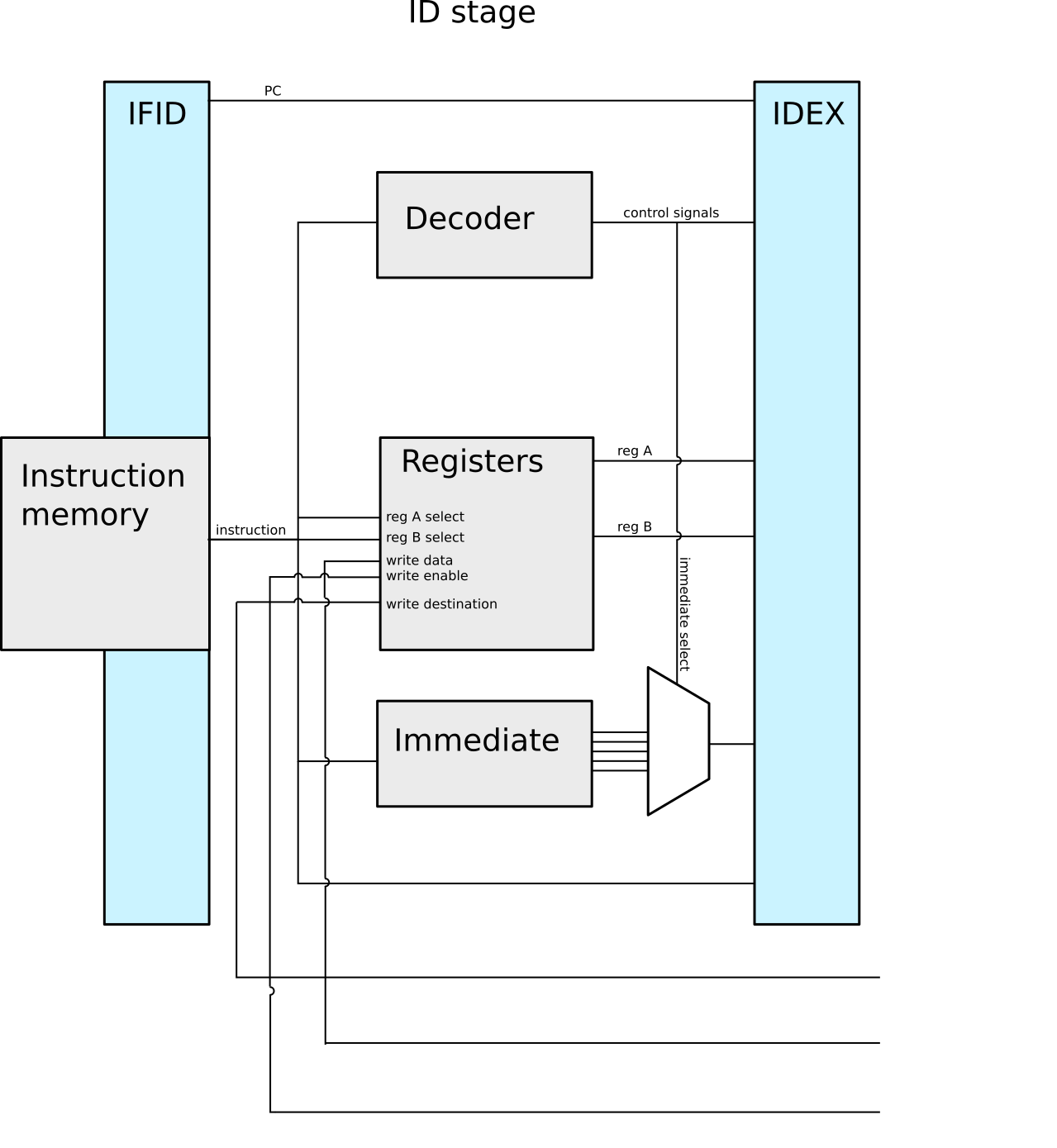
I would generally advice to do these on paper, but don't half-ass them.
Adding numbers
In order to get started designing your processor the following steps guide you to implementing the necessary functionality for adding two integers.
Info is progressively being omitted in the latter steps in order to not bog you down
in repeated details. After all brevity is ~the soul of~ wit
Step 0
In order to verify that the project is set up properly, open sbt in your project root
by typing ./sbt.sh (or simply sbt if you already use scala).
sbt, which stands for scala build tool will provide you with a repl where you can
compile and test your code.
The initial run will take quite a while to boot as all the necessary stuff is downloaded.
Step ¼:
In your console, type compile to verify that everything compiles correctly.
Step ½:
In your console, type test to verify that the tests run, and that chisel can correctly
build your design.
This command will unleash the full battery of tests on you.
Step ¾:
In your console, type testOnly FiveStage.SingleTest to run only the tests that you
have defined in the test manifest (currently set to forward2.s).
As you will first implement addition you should change this to the add immediate test.
Luckily you do not have to deal with file paths, simply changing forward2.s to
addi.s suffices.
Ensure that the addi test is run by repeating the testOnly FiveStage.SingleTest
command.
Step 1:
In order to execute instructions your processor must be able to fetch them.
In /kaholaz/TDT4255/src/commit/3b635be2dc5ba57dbd87ae872818f2c1004a6bd6/src/test/main/IF.scala you can see that the IMEM module is already set to fetch
the current program counter address (line 41), however since the current PC is stuck
at 0 it will fetch the same instruction over and over. Rectify this by commenting in
// PC := PC + 4.U at line 48.
You can now verify that your design fetches new instructions each cycle by running
the test as in the previous step.
Step 2:
Next, the instruction must be forwarded to the ID stage, so you will need to add the instruction to the io interface of the IF module as an output signal. In /kaholaz/TDT4255/src/commit/3b635be2dc5ba57dbd87ae872818f2c1004a6bd6/src/test/main/IF.scala at line 21 you can see how the program counter is already defined as an output. You should do the same with the instruction signal.
Step 3:
As you defined the instruction as an output for your IF module, declare it as an input in your ID module (/kaholaz/TDT4255/src/commit/3b635be2dc5ba57dbd87ae872818f2c1004a6bd6/src/test/main/ID.scala line 21).
Next you need to ensure that the registers and decoder gets the relevant data from the instruction.
This is made more convenient by the fact that Instruction is a class, allowing you
to access methods defined on it.
Keep in mind that it is only a class during compile and build time, it will be
indistinguishable from a regular UInt(32.W) in your finished circuit.
The methods can be accessed like this:
// Drive funct6 of myModule with the 26th to 31st bit of instruction
myModule.io.funct6 := io.instruction.funct6
Step 4:
Your IF should now have an instruction as an OUTPUT, and your ID as an INPUT, however they are not connected. This must be done in the CPU class where both the ID and IF are instantiated. In the overview sketch you probably noticed the barriers between IF and ID. In accordance with the overview, it is incorrect to directly connect the two modules, instead you must connect them using a barrier. A barrier is responsible for keeping a value inbetween cycles, facilitating pipelining. There is however one complicating matter: It takes a cycle to get the instruction from the instruction memory, thus we don't want to delay it in the barrier!
In order to make code readable I suggest adding a new file for your barriers, containing four different modules for the barriers your design will need.
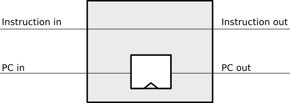
Start with implementing your IF barrier module, which should contain the following:
- An input and output for PC where the output is delayed by a single cycle.
- An input and output for instruction where the output is wired directly to the input with no delay.
The sketch for your barrier looks like this
Step 4½:
You can now verify that the correct control signals are produced. Using printf, ensure that:
- The program counter is increasing in increments of 4
- The instruction in ID is as expected
- The decoder output is as expected
- The correct operands are fetched from the registers
Keep in mind that printf might not always be cycle accurate, the point is to ensure that your processor design at least does something! In general it is better to use debug signals and println, but for quick and dirty debugging printf is passable.
Step 5:
You will now have to create the EX stage. Use the structure of the IF and ID modules to guide you here. In your EX stage you should have an ALU, preferrable in its own module a la registers in ID. While the ALU is hugely complex, it's very easy to describle in hardware design languages! Using the same approach as in the decoder should be sufficient:
val ALUopMap = Array(
  ADD    -> (io.op1 + io.op2),
  SUB    -> (io.op1 - io.op2),
  ...
  )

// MuxLookup API: https://github.com/freechipsproject/chisel3/wiki/Muxes-and-Input-Selection#muxlookup
io.aluResult := MuxLookup(io.aluOp, 0.U(32.W), ALUopMap)
As with the ID stage, you will need a barrier between ID and EX stage. In this case, as the overview sketch indicates, all values should be delayed one cycle.
When you have finished the barrier, instantiate it and wire ID and EX together with the barrier in the same fashion as IF and ID. You don't need to add every single signal for your barrier, rather you should add them as they become needed.
Step 6:
Your MEM stage does very little when an ADDI instruction is executed, so implementing it should be easy. All you have to do is forward signals.
From the overview sketch you can see that the same trick used in the IF/ID barrier is utilized here, bypassing the data memory read value since it is already delayed by a cycle.
Step 7:
You now need to actually write the result back to your register bank. This should be handled at the CPU level. If you sketched your processor already you probably made sure to keep track of the control signals for the instruction currently in WB, so writing to the correct register address should be easy for you ;)
If you ended up driving the register write address with the instruction from IF you should take a moment to reflect on why that was the wrong choice.
Step 8:
Ensure that the simplest addi test works, and give yourself a pat on the back! You've just found the corner pieces of the puzzle, so filling in the rest is "simply" being methodical.
Delivery
Once you are done simply run the deliver.sh script to get an archive.